





Tata Electronics targets December for its maiden wafer run, while the government doubles down with a fresh round of semiconductor approvals
The prolonged initiative undertaken by India for developing its domestic semiconductor industry is reaching a critical stage. The upcoming first ever production line of Tata Electronics in the Dholera Special Investment Region in Gujarat State is indicative of India’s efforts in the wake of recent clearance of fresh initiatives for the country’s semiconductor mission.
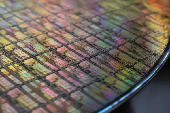
Close-up of a silicon semiconductor wafer showing etched circuit patterns
A Fab Finally Takes Shape
For a long time now, the Indian dreams of becoming a semiconductor superpower have been on paper. However, this is set to change with the Tata-PSMC venture in Dholera. This plant has been set up with a total investment of around Rs 91,000 crore. As per Union Minister Ashwini Vaishnaw, the production of the first wafers is set to start from December of this year, a development that will see the nation enter the real semiconductor production phase from the packaging stage.
The Dholera plant has been accorded special economic zone status and has been provided with an inland container depot, which shows the importance accorded to the venture by the government.
Semicon 2.0 Widens the Net
Parallel to the progress made at the fab, the Cabinet has also greenlit Semicon 2.0, which essentially extends the scope of the mission into a new phase with an outlay of over Rs 1.27 lakh crore. While the earlier phase was all about the establishment of fabs and assembly lines, the current phase emphasizes more the development of chips, specialty materials, manufacturing equipment, and IP in the ecosystem, which do not often come into focus when attention is centered only around factories.
The two new initiatives launched under this push include the setting up of an integrated fabrication and assembly line of compound semiconductors by Crystal Matrix Limited in Dholera to manufacture components for Mini/Micro-LED displays along with gallium nitride foundry services and outsourcing assembly and test facility in Surat by Suchi Semicon Private Limited, with an annual capacity to process more than one billion chips, for power electronics, automotive and industrial applications.
In total, these two add up to twelve approved semiconductor facilities across the nation in six states with committed investment of Rs 1.64 lakh crore.
Where India Stands Today
However, progress on the ground has been steady, if slow. As of August, three of the twelve commercial facilities that have received approval are now up and running. The Micron assembly and test facility at Sanand is one of the early successes, with the CG Power OSAT facility in the same industrial cluster following close behind, providing packaging services to automotive-grade quality standards.
Of course, it is important to acknowledge the extent to which progress has its limitations. Currently, India’s capabilities are limited to the mature nodes and packaging end of the industry, where memory chips and automotive-grade assembly work can be done, but not at the front end with cutting-edge logic chips used in AI accelerators and smartphones. Facilities capable of manufacturing chips in the sub-seven nanometer range are still several years off, with India expected to reach the cutting edge only after the next decade.
Why the Push Matters
This rush has its roots in the worldwide shortage of semiconductors in 2020 and 2021 and has revealed the high levels of dependency of the Indian economy on chips imported from abroad, especially in industries such as automobiles and consumer electronics. Even creating production capacities in the mature node stage makes them less vulnerable to any shortages, as well as giving them access to an additional source of chips produced domestically, rather than importing them from East Asia.
Another reason for expanding the production capacity is the potential for sales. According to estimates, the demand of the Indian market for semiconductors will reach the one hundred billion-dollar point before the end of the decade, stimulated by developments in the electric car industry and telecommunications, and consumer electronics production.
What Comes Next
Upcoming months will serve as the true test of whether this initiative’s momentum can be maintained. Should Dholera begin delivering its first wafers according to plan in December, this would signify a true milestone, as well as the evidence that the nation is capable of moving beyond component assembly toward production. The extent to which the ecosystem surrounding these facilities, from talent to specialized material providers, is able to keep up with the establishment of new fabs, will be the determining factor in how much of this investment will pay off.